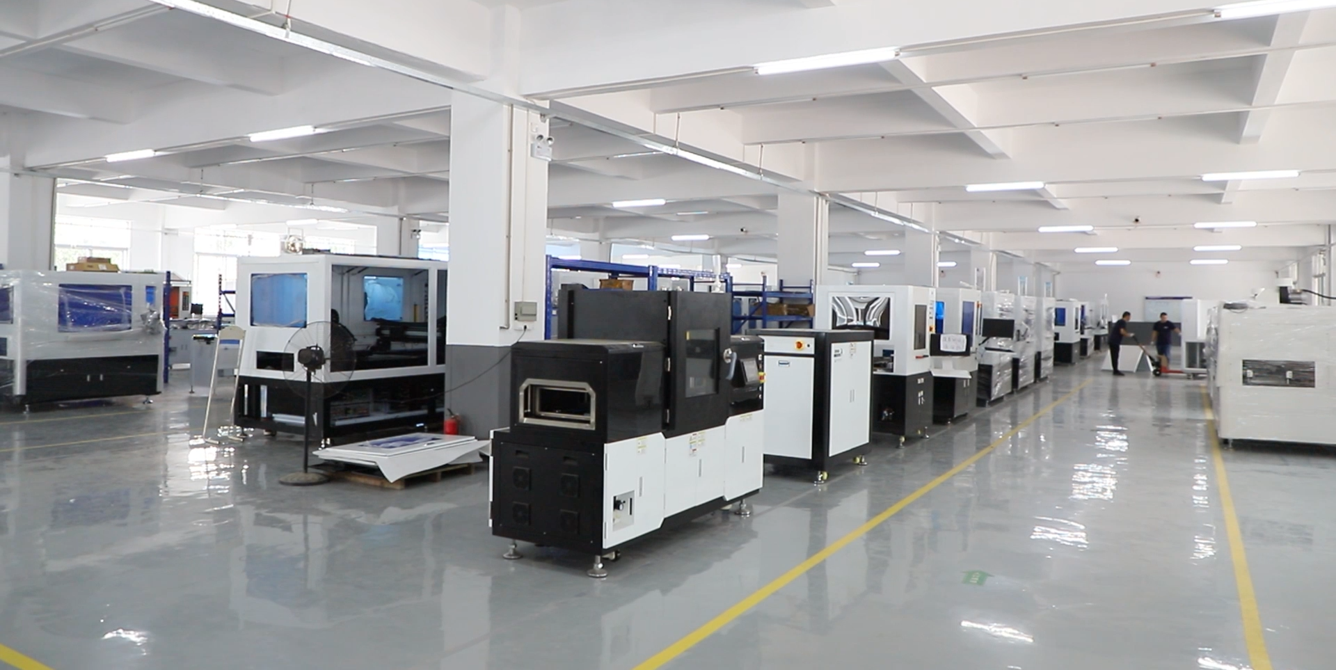
The working process of GOB LED encapsulation can be divided into three core stages integrating precision positioning, material filling, and curing technologies:
I. LED Chip Mounting and Pretreatment
- Precision Chip Alignment
LEDs are accurately positioned on PCB boards using SMT technology, ensuring spacing and layout compliance with design specifications.
- Surface Preparation
Plasma cleaning or chemical treatment removes oxidation layers and contaminants from PCB surfaces, enhancing adhesive bonding strength.

II. Encapsulation and Optical Enhancement
- Encapsulant Selection & Dispensing
Customized high-performance optical thermal adhesives (e.g., nano-scale materials) fill chip gaps through vacuum molding or dispensing processes, achieving light transmittance ≥95% and thermal conductivity >1.5 W/m·K.
- Thickness Control
Automated equipment maintains encapsulation layer thickness tolerance ≤0.05mm, preventing chromatic aberration or moiré patterns.
III. Curing and Protection Reinforcement
- Thermal/UV Curing
Thermal curing (80-120°C) or UV irradiation induces cross-linking polymerization, forming impact-resistant (≥50 kg/cm²) and salt spray-resistant (1,000 hours) protective layers.
- Surface Finishing
Post-curing grinding achieves surface roughness Ra≤0.1μm, with dual matte finishing enhancing color contrast by approximately 20%.
Key Advantages: Converts discrete LEDs into uniform surface light sources with 180° viewing angle, while delivering 30% reduction in blue light peak intensity for enhanced display performance and reliability.
 ×
×
